搜索此博客

2015年6月26日星期五

How to win your orders and clients

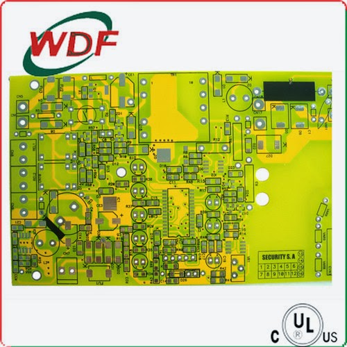
WDF-PCB-M-31,4 layer,wonderfulpcb.com


People who order PCB and PCBA from you are in different ways and different needs. So do how you know your client? Do you know what kind of clients they are and can you make a high quote to your clients?

Firstly, you should learn to know your customers. You’d better make a category. There are several kinds of customers. One is the factory which need your boards to make electronic products. This kind of clients are good for you. Because they are indeed asking for your products. Sometimes , if the customers are from rich country, such as Europe countries and USA, then you are lucky, you can quote for a higher price because they are care more about the quality and leadtime. The other one is a distributor who is care more about the money. Everytime they make a inquiry, then they would bargain with you to get a lower price. So these clients are hard to treat well. So we need more tips to fight against them. We may quote a higher price at first and give ourselves some room to reduce the price.

Before we make a quotation to our clients, we ‘d better make a survey on our clients. We can learn more about our clients if they have a factory and what products are they produced, how many pcb they would need in a year and the most important thing is which country are they from. We need to know the situation of the country in this competitive world. In other word, we should deeply know how is our clients.

I think if one can make some analyses before we make a quotation to our clients. We can hold our own advantage and make a good relationship with our clients. There is a proverb saying so: Opportunities will always be people who are prepared.

2015年6月3日星期三

PCB drilling


Holes through a PCB are typically drilled with small-diameter drill bits made of solid coated tungsten carbide. Coated tungsten carbide is recommended since many board materials are very abrasive and drilling must be high RPM and high feed to be cost effective. Drill bits must also remain sharp so as not to mar or tear the traces. Drilling with high-speed-steel is simply not feasible since the drill bits will dull quickly and thus tear the copper and ruin the boards. The drilling is performed by automated drilling machines with placement controlled by a drill tape or drill file. These computer-generated files are also called numerically controlled drill (NCD) files or "Excellon files". The drill file describes the location and size of each drilled hole.

Holes may be made conductive, by electroplating or inserting metal eyelets (hollow), to electrically and thermally connect board layers. Some conductive holes are intended for the insertion of through-hole-component leads. Others, typically smaller and used to connect board layers, are called vias.

When very small vias are required, drilling with mechanical bits is costly because of high rates of wear and breakage. In this case, the vias may be laser drilled—evaporated by lasers. Laser-drilled vias typically have an inferior surface finish inside the hole. These holes are called micro vias.

It is also possible with controlled-depth drilling, laser drilling, or by pre-drilling the individual sheets of the PCB before lamination, to produce holes that connect only some of the copper layers, rather than passing through the entire board. These holes are called blind vias when they connect an internal copper layer to an outer layer, or buried vias when they connect two or more internal copper layers and no outer layers.

The hole walls for boards with two or more layers can be made conductive and then electroplated with copper to form plated-through holes. These holes electrically connect the conducting layers of the PCB. For multi-layer boards, those with three layers or more, drilling typically produces a smear of the high temperature decomposition products of bonding agent in the laminate system. Before the holes can be plated through, this smear must be removed by a chemical de-smear process, or by plasma-etch. The de-smear process ensures that a good connection is made to the copper layers when the hole is plated through. On high reliability boards a process called etch-back is performed chemically with a potassium permanganate based etchant or plasma. The etch-back removes resin and the glass fibers so that the copper layers extend into the hole and as the hole is plated become integral with the deposited copper.

If you need expert PCB services, feel free to contact us at wonderful02@wonderfulpcb.com

2015年5月25日星期一

Some points should be noticed for etching


Reduce erosion and protrusion along the side to improve the etching factor. Produce sudden lateral erosion along. Printed in the etching solution is usually longer, (or use the old vacillating etching) the more serious side etch. Lateral erosion seriously affect the accuracy of printed conductors, would severely undercut the production of fine wires become impossible. When the lateral erosion and sudden decreases along the etching coefficient is increased, a high etching coefficient indicates the ability to maintain the thin wire, so close to the wire after etching artwork size. Plating etching resist either tin - lead alloy, tin, tin - nickel alloy or nickel, can cause sudden excessive wire along a short circuit. Because projecting along easily broken down, between two points of an electrical wire bridge.

Board and the board to improve the consistency between the etch rate. Board in a continuous etching, the etching rate is more consistent, more uniform etching of the board can be obtained. To meet this requirement, must ensure that the etching solution in the whole process of etching remain etched in the best condition. This requires selection easy to regenerate and compensation, the etching rate of the etching solution is easy to control. Used to provide constant operating conditions and parameters of the various solutions can be automatically controlled processes and equipment. By controlling the amount of dissolved copper, PH value of the solution concentration, temperature, solution flow rate uniformity (spray nozzle and a nozzle system or swing) or the like.

Improve the safe handling and etching thin copper foil and the ability of the etching thin laminate multilayer thin laminate inner layer so when the board is easy to wound on rollers and transfer wheel and cause waste. Therefore, the etching of the inner plate device must guarantee smooth, reliably handle a thin laminate. Many equipment manufacturers in the etching machine gears or rollers attached to prevent the occurrence of such phenomena. A better approach is to use an additional Teflon coated vacillating envelope sent as a thin plate supports. For thin foil (e.g., 1/2 or 1/4 ounce) etching, must guarantee not to be scratched or scratched. Stand like a thin copper foil etching 1 ounce copper on the mechanical drawbacks, sometimes more intense vibrations are likely to scratch the foil. 

For more details and technical supports, please feel free to contact us.

2015年5月4日星期一

What are Aluminum PCBs


Also known as metal base PCBs, aluminum based PCBs comprise metal based laminates that are covered by copper foil circuit layers. They are constructed utilizing alloy plates, which consist of a combination of Aluminum, Magnesium, and Silumin (Al-Mg-Si). These PCBs are known for their beneficial features such as electrical insulation, good thermal potential, and high machining performance.

Aluminum PCBs differ slightly from general PCBs. The structure of this PCB comprises:
Ø Base Layer: This layer consists of an aluminum alloy substrate. The use of aluminum makes this PCB an excellent choice for PTH technology. Holes can be cut, punched, or drilled to the requisite sizes.
Ø Insulation Layer: While the base layer is certainly important, the thermal insulation layer is a critical component of this PCB. It consists of a special ceramic polymer, which has excellent viscoelastic properties and thermal resistance. The insulation layer also protects the PCB from thermal and mechanical stresses.
Ø Circuit Layer: This layer comprises the copper foil mentioned earlier. Generally, PCB manufacturers utilize thick copper foils, which can range from 1oz to 10oz.

There are certain materials and processes that can be used to augment the performance of the PCB. These include gold plated HAL, lead free RoHS assembly processes, immersion gold silkscreen, and OSP anti-oxidation processes.

While aluminum PCBs consist of the same width and thickness as FR4 PCBs, the alloy plate allows the PCB to increase its conductivity to 2.0. Also, it can carry higher currents and withstand up to 4,500 volts of electricity.

If you need expert PCB assembly service, feel free to contact wonderful02@wonderfulpcb.com

2015年4月24日星期五

PCBA Industry News

1.Drilling and electroplating
If production is a multilayer PCB, and containing buried hole or blind hole, each layer board must be bored with first plating before bonding. If you don't pass this step, then can't connect each other.
After by machine equipment according to the requirements of drilling borehole Kong Bi inside must go Through electroplating (Plated Through Hole technology, Plated - Through - Hole technology, PTH).After Kong Bi internal make metal processing, can make the internal lines of each layer can be connected to each other. Before starting the electroplating, must first clear hole of sundry. This is because the resin epoxy compound after heating will produce some chemical change, and it can cover internal PCB layer, so need to clear out. Remove and electroplating movements will be completed in the chemical process.

2. Multilayer PCB pressing
each single layer must be pressing to make sandwich plate. Pressing action including adding insulation between the layers, and fastened to each other. If there is through several layers of guide hole, then each layer must be repeated. A multilayer wiring on the outside of the two sides, is often only after a multilayer pressing processing.

3. Treatment resistance welding layer, surface screen printing and gold finger plating
Next resistance welding paint coverage on the outermost wiring, so the wiring will not come into contact with the outside plating parts. Screen printing surface is printed on it, to mark the location of the various parts, it will not be able to cover at any wiring or gold finger, otherwise may reduce solder ability or the stability of the current connection. Gold finger parts usually gold plating, which, when inserted into the expansion slot to ensure high quality of the current connection.

4. Test
to test whether there is a short circuit or open rigid PCB can use optical or electronic means testing. Optical methods using scanning to find out the defects of each layer, electronic testing is usually with fly needle detector (Flying Probe) to check all the connections. Electronic testing in search of short circuit or open circuit is precise, but the optical test cans more easily detected incorrect gaps between the conductors.

2015年4月15日星期三

Lead Time of PCB Assembly

Before a new electronic product can get accepted on the market, there are many things need to do. First of all, you should have a new correct design. How to know whether your design is correct and perfect without any problem? Be careful on the below steps, you’re probably going to need them in the near future.

To verify your PCB design, engineers usually will find some companies to make some PCB prototypes. For example, if you PCB is a double-sided PCB, it will spend about 5-7 days for a real PCB manufacturer. But you just get a bare PCB, without any components on it. So how could it verify the design? The answer is not. It can’t check the problems in your design. You need to have a complete board with all necessary parts on it.

You may think, offer you the bill of materials, the manufacturer can buy them for you. Yes, it usually works if they do have a professional purchase department. If not, you are going to buy all the components by yourself. It sounds crazy trouble. Yes it is. So usually the designer wants PCB and components assembly. It takes long time to have all the components, because some integrated circuits will need import from overseas. It does need a lot of time, usually 3 weeks. So the lead time of PCB assembly will be probably the lead time of all components? Nope, you should never forget the time for assembly. It won’t last one week if the BOM list it not so complicated.

Now you’ll know the whole lead time for PCB assembly. It really depends on the components source of your purchase department. They fast, lead time short. Otherwise, they slow, lead time long.

So if you are considering making a PCB prototype and assembly, think about the lead time. Prepare enough time in your time schedule for it, figure out a testing method for it when you have it. Most important thing is that it may need several times for prototyping. You will find problems in your design from each prototype. It takes money. Now go getting all the potential costs approved by your accounts in advance.

When it is time for finding a manufacturer, consider manufacturers in Shenzhen, China. They have done offering these kinds of services professionally for years. You want some good companies to be recommended? WONDERFUL PCB LIMITED is not a bad choice.

If you need expert PCB assembly service, feel free to contact wonderful02@wonderfulpcb.com.

PCB Industry

At present, Chinese production of electronic circuits, and printed circuit industry sales accounted for 44 percent of the global total; China printed circuit board equipment, raw materials, sales and production also remain the world's first. Despite the good momentum of development, many exhibitors participating CPCASHOW has said that due to the recent influx of a large number of PCB industry areas, capacity expansion is serious, resulting in a vicious competition intensified. In addition, the continued growth of smart terminals and emerging markets, driven by significantly increasing the demand for HDI, FPC, etc., but also stimulate the industry investment to expand plant expansion, further intensified price competition.

I found that many domestic exhibitors showcasing high-order HDI, IC, buried blind PCB, FPC, high-end products, such as multi-layer FPC, PCB manufacturers have indicated that many domestic with international advanced manufacturing PCB comparable.

Production capacity expansion, high degree of product homogeneity, leading PCB price pressures. Price war intensified, most industry struggling to cope.

How to deal with a price war? I found a positive innovation in the field show exhibitors are booming popularity. Visible on the product technology upgrades, technological innovation will help blaze a new trail in the price war. In addition, to improve product competitiveness, increase product functionality and value, so that enterprises break free from the mire of product homogeneity, but also to important initiatives.

When it is time for finding a manufacturer, consider manufacturers in Shenzhen, China. They have done offering these kinds of services professionally for years. You want some good companies to be recommended? WONDERFUL PCB LIMITED is not a bad choice.

If you need expert PCB assembly service, feel free to contact wonderful02@wonderfulpcb.com.

2015年4月13日星期一

Prototype PCB Necessity and Benefits(1)----Wonderful PCB (hk) Limited

Author: Jodie
PCB prototype plays a very important role in the creation and design of PCB (Printed Circuit Boards). The design of the PCB does not depend on single elements rather depends on variety of elements which needs expertise and testing for several times. And prototype gives you the opportunity to check your product before production. Actually, we can say that the design depends on indistinct set of necessities. This is produced to define the required functions for the electrical and mechanical products. And the prototype helps to fulfill these needs by giving you a chance for proving your design.
The designers include all the required functionalities those can fit in the board. As regarding to the requirements, the board changes its shape. Sometimes it's large with the extensive requirements. And sometimes it's small with fewer requirements. Again many things are needed to make a pcb prototype of production stage. Among them, functionality with reliability is a must. The complexity and functionality determines the required number of layers. Some board consists of only two layers as they have less functionality and some have even more than 32 layers for their complexity and high functionality. And the size also differs a lot. As the board has to sit perfectly into its desired system, it must be made in the perfect shape. The tolerance is also a factor as the layers and copper traces certainly depend on it. Most PCB has a design with a tolerance that makes the layers and copper traces even more critical. As they are designed with highly tight tolerances, they are made highly integrated. And this integrity sometime causes some critical problems. So, it must be checked carefully for the accuracy. The voltage must be moderate with the application and the signals must also be clean. Again, the surface components must meet the required tolerance. And after considering all these respects, the developed first board is called the prototype. These are developed for testing. They are mainly made depending on the number of testing required. After the testing is completed, the production begins with the design.

2015年4月12日星期日

Several classification of flexible printed circuit board

 Author:Faith Fan

At present, mainly has the single side, double side, multilayer flexible circuit and flexible circuit board just four.


(1) single flexible plate is the lowest cost, when the Aluminum pcb for electrical demand is not high.When single wiring, should choose single flexible plate.It has a layer of chemical etching of conductive graphics, in the flexible conductive graphics layer on the surface of the insulating substrate for rolled copper foil.Insulating base material can be polyimide, polyethylene terephthalate, aromatic polyamide fiber resin and PVC.


(2) double flexible plate is on the two sides each have a layer of insulating base film etching made of conductive graphics.Metallized hole to both sides of the insulation materials connection form a conductive path, in order to meet the deflection design and use of the function.While covering film can protect the single and double wires and components placed.


(3) multilayer flexible plate is a level 3 or more layers of single sided or double sided laminated flexible circuit together, through the drill away L form hole metallization, electroplating, the formation of a conductive path between different layers.So, do not need to adopt the complex welding process.Multilayer circuit in higher reliability, better thermal conductivity and convenient assembly has huge function differences in performance.When designing the layout, assembly shall be taken into consideration, layer number and size of flexible influence each other.


(4) the traditional just flexible plate is made from rigid and flexible substrate has a choice of formation pressure together.Structure closely to metallization away L form electrical connection.If a PCB is, opposite element, just flexible plate is a good choice.But if all the components are on one side, selects the double flexible plate, and on the back of the laminated layer on FR4 reinforced material, will be more economic.


Hybrid structure is a kind of sandwich plate, flexible circuit conductive layer made of different metals.A eight layer plate using FR - 4 as inner layer medium, the use of polyimide as outer medium, out from three different direction of the main board, lead each wire made of different metals.Constantan alloy, copper and gold as independent lead, respectively.This kind of hybrid structure is mostly used in electrical signal conversion and is quite harsh relationship and performance of heat transformation of low temperature circumstances, is the only feasible solution.


Even through the design and how easy it is to evaluate the total cost, in order to achieve the best performance/cost ratio.

2015年4月10日星期五

PCB Replacement and Repair

The world is changing and technology is always changing too! But sometimes there are certain components which need some minor tweaks and changes to last even longer throughout the years. This can even happen with a client's manufactured electronic products when they need to be upgraded to a newer manufactured device.

When this happens, your manufacturer can help with the entire process of helping all of your clients to prevent sluggish PCB systems. However, there are other reasons why a PCB needs to be repaired, other than having to upgrade the entire system.

Wonderful PCB (HK) Limited is a professional PCB manufacturer with assembly line in house. It provides high quality PCB with good after-sale service. In face of complainant from clients, Wonderful PCB provides completed after-sale service including PCB replacement or repair.

Saving Time, Money & Repairing Defects

When you're going to ship out huge batch orders of units, sometimes taking the extra time to keep account of all of the components and making sure that every single component are finely assembled on the PCB board. And make sure every single one doesn't have a defect which can be very time consuming. However, you can save time from having to recall certain parts or dealing with defunct PCBs by Wonderful PCB when they can correct a design flaw to make sure PCB-repair the system isn't running slow.

This is also good for you, because it means your own clients utilizing PCBs won't be complaining about sluggish systems that can cost them time and money too. You can also implement cost effective solutions when a PCB needs to be repaired, which can mean not having to replace an entire batch order and do a complete redesign simply because of a minor defect that can be repaired by the manufacturer.

New Software, New Repairs

When your PCB components and software are due for a brand new update, please don't worry more about it: Wonderful Quick turn PCB can take care of everything. Sometimes software on the PCB can become slow and sluggish when it is new and the platform it is running on is older than the software itself, making it frustrating for all parties involved.

You or your clients using the PCB components need to stay up with all of the latest software, especially when everything is becoming so fast paced in the technology industry as is. PCB board repair can ensure that everything is fast, highly responsive, and in working order with the best components available on the market.

However, PCB repair and replacement which does mean that the entire batch order will need to be repaired in order to ensure that the software continues to run seamlessly and smoothly. This can take some time to do with bigger orders, but like mentioned earlier, the investment in PCB repair services creates better time management in the long run.

2015年4月8日星期三

What’s PCB?

A PCB is a printed circuit board. It is mainly used in electronic industry.

A PCB serves two purposes in the construction of an electronic device; mount the components and provides the means of electrical connection between components.

A PCB starts as a thin, non-conducting sheet of material. The most common material used is a glass fiber epoxy laminate material. A thin layer of copper is then chemically deposited on each side of this material. The next step is to "print" the connection diagram onto the PCB. In the very early days of electronics, these connections were done with wires. That’s why PCB is also referred to printed wiring boards. The "printing" is usually done by photographically, transferring the image to the board. This image is "printed" with an acid resistant material.

Next, the Rigid-flex pcb is put into an acid bath. The acid bath removes the copper from the board, excepting the areas protected by the resistant material. This process leaves the connections or wiring "printed" on the PCB. Next, holes are drilled in the board to allow the components to be mounted to the board and the PCB itself to be mounted to the case protecting the electronics. Finally, a protective coating is applied to the board to prevent corrosion of the copper traces.

It is possible to make     PCB to any number of layers by repeating the process above and laminating the resulting boards into a single PCB. The circuit board inside of the computer on which you are reading this document has a minimum four layers and is more likely to be an eight or even 12 layer PCB.

It is also more common now for parts to be soldered directly to the board, eliminating the need for holes into which leads (wires) from the components must be inserted. A component soldered to the board is logically called a surface mount component, and the board is a surface mount PCB. This technique allows a large increase in the number of components to be mounted on the same PCB, or the same number of components to be mounted on a much smaller one. However, surface mounting also requires better quality control on the manufacture of the PCB.
A PCB is now used in almost every electronic product available. It is by far the most common method currently used to connect and assemble the components of almost any electronic device.

2015年4月7日星期二

Fr-4 material

FR-4 is a flame retardant material level code, represent the meaning of the resin material undergoes combustion state must be able to extinguish a material specification, it is not a material name, but a material level, so the current general circuit boards used in FR-4 grade materials have a lot of types, but most are based on a so-called four-function (Tera-Function) of an epoxy resin with filler (Filler) and glass fibers made ​​of composite materials. FR4 substrate portion, the most widely used family on a printed circuit board substrate is a glass fiber epoxy laminate. FR4 substrate is a standard part of most of the material has a higher number (such as some portion of FR4 substrate FR4 substrate 06, 08) has a higher temperature coefficient and a low dielectric constant. Part FR4 substrate with a starting Tg 140 ° C, Tg FR4 substrate 06 parts of 170 degrees, and when you move up the family, the temperature increases.

FR-4 epoxy glass cloth laminated sheet, depending on the use of different industries generally known: FR-4 Epoxy Glass Cloth, insulation board, epoxy boards, epoxy boards, brominated epoxy boards, FR-4 , glass fiber, glass fiber board, FR-4 reinforcement plate, FPC reinforcement plate, flexible circuit board reinforcement plate, FR-4 epoxy board, fire-retardant insulation board, FR-4 laminates, epoxy board , FR-4 light board, FR-4 fiberglass board, epoxy glass cloth laminated sheet, epoxy glass cloth laminated board, circuit board drilling pad. Main technical characteristics and applications: electrical insulation [1] stable, good flatness, smooth surface, no pits, the thickness tolerance standard, suitable for high-performance electrical insulation requirements for products, such as FPC reinforcement plate, PCB drilling plate, glass rings, glass fiber carbon printed potentiometer, precision planetary gear (wafer grinding), precision test plates, electrical (electrical) equipment insulation stays partitions, insulation plate, transformer insulation boards, electrical insulation , grinding gears, electronic switches insulation panels.

Epoxy fiberglass cloth boards, the most widely used product model for FR-4, the electronic product installation techniques and PCB technology development needs, and the emergence of high Tg FR-4 product.

How to get more and more orders from customers

In today's condition of information explosion, the business is more and more difficult. Especially in the global financial crisis period, feelings will be deeper. Therefore, in this adverse environment and more fierce competition, how to get orders is very important.
Try to improve overall quality, the higher of the overall quality, the more appealing.
We often encounter a situation: on the same question, someone will find very excellent answer, his clarity, logic, feasibility are all above the crowd. Why? Because of the high overall quality. Therefore, We must pay attention to learning, attention to the accumulation of experience, attention to learn from the experience, pay attention to constantly improve our self-serving to speak and act. As the saying goes: "do business must first learn how to be a good man",  in fact, it is not only integrity, more important is to have a high ideological and cultural taste. So when in contact with the customer, it will make people feel your outstanding, they will admire and believe you before do business with you. Thus, after several contacts and then the customer and you will tend to become friends, and slowly became "buddies child." Then there will be a lot of business after that.
Written by Shirley Xia from Wonderful PCB company
Wonderfulpcb is an experienced PCB board manufacturer,provide various of PCB board,Aluminum pcb,Flexible pcb,Rigid-flex pcb,Multilayer pcb,and PCBA at competitive prices.

2015年4月1日星期三

Wonderful Limited PCBA assembly

This month Wonderful PCB is going to make a new website to introduce a totally improved PCB factory from every side. Our products printed circuit board and PCB assembly, our service, our capability and so on. My team work is writing the PCB application such as mobile phone PCB, digital PCB, game PCB, LED PCB, USB PCB, PC-computer PCB, PCB Assembly, PCB prototype, flexible PCB, rigid PCB, rigid-flex PCB, special technology PCB. The other team’s task is description the material and layers we can do. There are having more than ten material for printed circuit board for example, aluminum material, FR4,ceramic,rogers,Isola, FR1, FR2, high frequency, CEM1,CEM3, copper material. The printed circuit board layers we make is from 1layer to 28layers.

PCB board assembly
ODM PCBA Services:
1.PCB assembly
2.Component purchase
3.SMT Machine of SIEMENS SIPLACE
4.Enclosure design&produce

OEM/ODM/EMS Services for PCBA manufacturer:
1. PCBA, PCB assembly: SMT & PTH & BGA
2. PCBA and enclosure design
3. Components sourcing and purchasing
4. Quick prototyping
5. Plastic injection molding
6. Metal sheet stamping
7. Final assembly
8. Test: AOI, In-Circuit Test (ICT), Functional Test (FCT)
9. Custom clearance for material importing and product exporting

PCBA Capacity:
SMT: 2,000,000 solder joints per day
DIP: 300,000 joints per day
SMT Production Flow:
Material Receiving → IQC → Stock → Material to SMT → SMT Line Loading → Solder Paste/Glue Printing → Chip Mount → Reflow → 100% Visual Inspection → Automated Optical Inspection (AOI) → SMT QC Sampling → SMT Stock → Material to PTH → PTH Line Loading → Plated Through Hole → Wave Soldering → Touch Up → 100% Visual Inspection → PTH QC Sampling → In-Circuit Test (ICT) → Final Assembly → Functional Test (FCT) → Packing → OQC Sampling → Shipping

Requested information for PCB assembly:
1. Gerber file of the bare PCB board
2. BOM (Bill of material) for assembly
To short the lead time, please kindly advise us if there is any acceptable components substitution
3. Testing Guide & Test Fixtures if necessary
4. Programming files & Programming tool if necessary
5. Schematic if necessary

Sophie Deng
_______________________________________
Wonderful PCB Limited
NO.32A,Building NO.1, XianDaiC hengHuaTing,ChuangYeRoad|NanShan District,ShenZhen City 518054|  China  T +86-755-86229518-806 | F  +86 755 2607 3529|  e  wonderful08@wonderfulpcb.com |
w  www.wonderfulpcb.com  | Skype:wonderful-07   |                                                   
Welcome to our trading shows:
1.Booth: L32,Expo Electronic 2013,Apr.10-12th in CROCUS EXPO,Moscow,Russia
2.Booth: 11J36, HK Global sources  Apr.12-15th, 2013 Asia World-Expo, Hong Kong
3.Booth: 9J35, HK Global sources Oct.12-15th,2013 Asia World-Expo, Hong Kong
4.Booth: 70206, CES  2014  Jan,8th-11th in Las Vegas, USA

Knowlage Of Printed Circuit Board

     Electronic products function depends on the correct interconnected electronic components, most of these components are interconnected based on the circuit board welding. Circuit board welding in the assembly of electronic products, has been playing an important role. There are many connections even if the current technology, but the circuit board welding remained dominant.

     Circuit board welding is an important part of electronic technology. Proper design and good solder process (ie, circuit board soldering process), is the key factor for reliable soldering. The so-called "reliable" refers to all the properties of the solder joints only when the product has just produced as required, but also throughout the life of electronic products, and should be guaranteed to work correctly.
   Although all of the physical-chemical principles of welding process is the same, but for soldering electronic circuits and has its own characteristics, i.e., miniaturization and high reliability, which is consistent with the characteristics of electronic products. Circuit board welding quality will be affected by many factors. Funds such as the type of material and its surface is, the type and thickness of the coating, processing technology and methods, surface condition before welding, soldering components, welding, soldering temperature and time are base metal welding gap size, flux type and performance, welding tools. Important reason for not being among the internal structure of the metal oxides and lead solder components lead compounds the situation is affecting the surface leads solderable, but also affect the surface of the oxide PCB pad solderability main reason.

     Using tin-lead soldering tin-lead solder is called, referred to soldering, the mechanism is: will solder in the solder process, weldment and copper under the action of heat welding, weldments and copper does not melt, the solder is melted and welded surface wetting rely weldments asked two copper atoms and molecules to move, thereby causing diffusion between the metal and the weld is formed between the copper alloy layer of a metal member, and to connect the copper foil and the weldment together, they get solid and reliable solder joints, the above process is the role of the physical-chemical processes each other.

    When the solder and welding weldment joint is heated to welding temperature, melting the solder does not melt weldment. Forming welding solder wetting rely molten state welding surface, resulting in the metallurgical, chemical reaction to form a bonding layer, to achieve a combination of the weldment. Lead-tin solder melting point below 200 ℃, suitable for connecting semiconductors and other electronic materials. Simply heating tools and materials can be processed, less investment. Joints have sufficient strength and electrical properties. Soldering process reversible, easy desoldering
Sophie Deng
_______________________________________
Wonderful PCB Limited
NO.32A,Building NO.1, XianDaiChengHuaTing,ChuangYeRoad|NanShan District,ShenZhen City 518054|  China  T +86-755-86229518-806 | F  +86 755 2607 3529|  e  wonderful08@wonderfulpcb.com |
w  www.wonderfulpcb.com  | Skype:wonderful-07   |                                                   
Welcome to our trading shows:
1.Booth: 9J35, HK Global sources Oct.12-15th,2013 Asia World-Expo, Hong Kong
2.Booth: 70206, CES  2014  Jan,8th-11th in Las Vegas, USA